
Behind every electronic innovation lies a fundamental truth: the performance of any system is only as strong as the components that drive it. Among these, the integrated circuit stands as the brain of modern electronics, translating code into action, processing signals into information, and enabling the functionality that defines today’s devices . HONTEC, a leading manufacturer of printed circuit boards serving high-tech industries across 28 countries, combines precision PCB manufacturing with comprehensive component intelligence to support the complete electronic ecosystem—including the sourcing, selection, and integration of integrated circuit components from industry leaders like NXP.
NXP Semiconductors has established itself as a premier provider of high-performance mixed-signal and security solutions, with a product portfolio that spans microcontrollers, processors, automotive chips, and wireless connectivity solutions . The company's legacy, originating from Philips' semiconductor division, has evolved into a comprehensive offering that addresses the most demanding applications in automotive, industrial IoT, mobile, and communication infrastructure markets . When engineering teams select NXP components, they gain access to:
- Automotive-Grade Solutions: The S32 automotive platform delivers scalable architecture for ADAS, vehicle networking, and powertrain applications, meeting ISO 26262 ASIL D safety standards
- Arm-Based Processing Power: From Cortex-M microcontrollers to Cortex-A application processors, NXP offers a broad performance range supported by the MCUXpresso development ecosystem
- Industry-Leading Security: EdgeLock secure elements and SmartMX controllers provide Common Criteria EAL 6+ certified protection for IoT and payment applications
The relationship between an integrated circuit and the board that hosts it is symbiotic. The finest NXP processor will underperform on a poorly designed substrate, and the most advanced PCB cannot compensate for an improperly selected component. This understanding drives HONTEC to offer integrated solutions that consider the complete system rather than isolated elements. Located in Shenzhen, Guangdong, HONTEC operates with certifications including UL, SGS, and ISO9001, while actively implementing ISO14001 and TS16949 standards [citation:URL].
NXP application notes emphasize that proper PCB design is essential for maximizing IC performance . HONTEC engineering team applies these principles to every project:
- Layer Stacking: For high-speed NXP processors, four-layer or six-layer PCBs with dedicated ground and power planes are recommended to maintain signal integrity
- Trace Routing: Right-angle bends in traces cause radiation and impedance changes. HONTEC routes signals with 45-degree corners or rounded bends to minimize reflections
- Ground Plane Design: A single, continuous ground plane is recommended for NXP microcontrollers—splitting ground planes for analog, digital, and power pins can degrade performance
NXP microcontrollers require careful crystal oscillator circuit design for accurate clock generation . HONTEC follows these guidelines:
- Placement: Crystals must be placed as close as possible (within 20mm) to oscillator input and output pins
- Trace Length: Oscillation circuit traces should be as short as possible and must not cross other signal lines
- Load Capacitors: External load capacitors should share a common ground plane, with values fine-tuned based on actual board layout
- Ground Pattern: A ground pattern should be laid out directly under the crystal unit, with no other signal lines crossing that area on multi-layer boards
- PMIC Integration: NXP offers scalable power management ICs and system basis chips for automotive and industrial applications
- Decoupling Capacitors: Proper placement of bypass capacitors is essential to prevent voltage ripple that causes logic errors [citation:URL]
- Thermal Management: HONTEC advises on copper pour strategies, thermal via placement, and heatsink attachment methods [citation:URL]
HONTEC maintains assembly capabilities tailored to the unique requirements of NXP IC components:
- Solder Paste Stencil Design: For fine-pitch NXP packages, stencil thickness and aperture geometry are optimized to achieve consistent solder volume across all connections
- Reflow Profiling: Thermal mass of NXP packages is considered to ensure all solder joints reach proper temperature without damaging thermal gradients
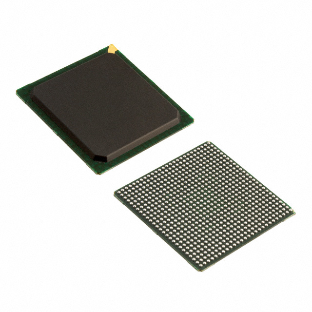
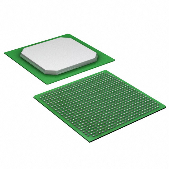
- X-Ray Inspection: For BGA packages, X-ray inspection verifies uniform solder ball collapse and acceptable void limits
- Moisture Control: HONTEC maintains controlled humidity environments for moisture-sensitive NXP components, applying baking processes when necessary
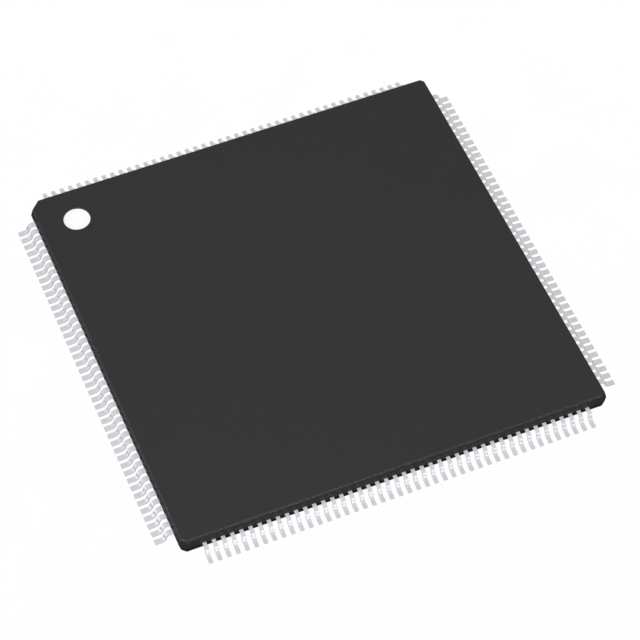
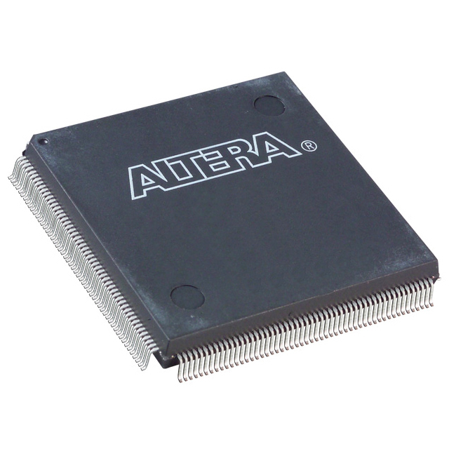
- Automated Optical Inspection: For quad flat packages, confirms lead coplanarity and solder fillet formation
- In-Circuit Testing: Verifies that NXP components respond to boundary scan commands
- Power Supply Verification: Ensures voltages reach components within specified tolerances
Selecting the right NXP integrated circuit involves balancing electrical performance, availability, cost, and long-term lifecycle considerations. The process begins with defining functional requirements—operating voltage, current consumption, clock speed, I/O count, and thermal characteristics. HONTEC recommends evaluating the manufacturer's production status, as components can face allocation challenges or end-of-life notices. Package type represents another critical consideration; BGA packages offer high I/O density but require advanced assembly capabilities, while QFP packages provide easier inspection and rework. Operating temperature range must align with the intended application environment, with industrial and automotive designs requiring extended tolerance beyond commercial grades. The NXP portfolio offers solutions for every requirement, from the ultra-low-power LPC series to the high-performance i.MX applications processors. HONTEC engineering team provides guidance during the design review phase, helping clients evaluate component selections against manufacturing capabilities. For designs where availability presents challenges, HONTEC offers alternative sourcing recommendations and can advise on pin-compatible substitutions that maintain design functionality while improving supply chain reliability.
The relationship between an NXP integrated circuit and the board that carries it is fundamentally interdependent. An NXP processor can only perform to its specifications if the PCB provides adequate power delivery, signal integrity, and thermal management. Power distribution network design directly affects IC performance; insufficient decoupling capacitance or improper placement of bypass capacitors can introduce voltage ripple that causes logic errors or timing violations. For high-speed NXP components, impedance-controlled traces are essential to maintain signal integrity and prevent reflections that corrupt data transmission. NXP application notes specify that high-speed signals must be routed above a solid, unbroken ground plane, and that floating metal shapes near microcontroller pins should be eliminated . Thermal management represents another critical factor; HONTEC advises clients on copper pour strategies, thermal via placement, and heatsink attachment methods that ensure the integrated circuit operates within its specified junction temperature. Ground plane design influences both signal integrity and electromagnetic emissions, with continuous reference planes providing the low-inductance return paths that high-speed ICs require. HONTEC manufacturing processes support these design requirements through tight impedance control, precise via formation, and advanced surface finishes that ensure reliable solder joint formation.
NXP integrated circuit assembly requires specialized processes that differ significantly from discrete component placement. HONTEC maintains assembly capabilities tailored to the unique requirements of NXP IC components. Solder paste stencil design receives particular attention for integrated circuit packages with fine-pitch leads or BGA configurations, with stencil thickness and aperture geometry optimized to achieve consistent solder volume across all connections. Reflow profiling considers the thermal mass of the NXP package itself, ensuring that all solder joints reach the appropriate temperature without exposing the component to damaging thermal gradients. For BGA NXP packages, X-ray inspection verifies that all solder balls have collapsed uniformly and that no voids exceed acceptable limits. Automated optical inspection for QFP packages confirms lead coplanarity and solder fillet formation. Electrical testing extends beyond basic continuity to include in-circuit testing where possible, verifying that the NXP component responds to boundary scan commands and that power supply voltages reach the component within specified tolerances. HONTEC maintains controlled humidity environments for moisture-sensitive NXP components, with baking processes applied when necessary to prevent popcorning during reflow. This comprehensive approach ensures that NXP integrated circuit components are assembled reliably and verified thoroughly before products move to final system integration.
HONTEC brings decades of experience in PCB manufacturing to bear on the complete electronic assembly process, supporting clients with integrated solutions that encompass board fabrication, component sourcing, and assembly services. The combination of advanced PCB fabrication, comprehensive component intelligence, and responsive customer service makes HONTEC a valued partner for engineering teams seeking reliable electronic solutions.
- Global Delivery: HONTEC partners with UPS, DHL, and world-class freight forwarders to ensure efficient global delivery
- Responsive Communication: Every inquiry receives a response within 24 hours, reflecting a commitment to responsive partnership
- Quality Certifications: UL, SGS, ISO9001, with ongoing implementation of ISO14001 and TS16949 standards [citation:URL]